 |
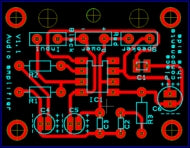
Software is used to create the board. This software allows parts to be added and connected together. Additional text and holes can be added to the board. The data is then exported as ‘gerber’ data, this is a list of shapes and their co-ordinates. There is a file for the copper wires (bottom), the identification (top), the solder resist (bottom), the drill holes and the board outline. We then put up to 60 boards together to make a larger panel with a mixture of different boards. This allows more of the same type of board to be made and is more cost effective. |
 |
A number of boards are stacked together and loaded in to the drilling machine. On the top and bottom of these boards is a sacrificial sheet of aluminium, used to make sure the holes are clean. The machine uses the rack of drill bits (right of picture), these are automatically optically checked for size and loaded into the drill. The drill moves about the board drilling holes, once all the holes of a particular size have been drilled the drill bit is changed for the next drill size. The machine can detect broken drill bits and automatically discards drills after a preset number of holes have been drilled and just before they become blunt. |
 |
To etch the copper off the boards a mask is required. This is a sheet of acetate that is printed with the tracks on the board. The machine shown on the left is only the finishing part of the printer. Behind the wall in a dark room is the main printer, which prints the acetate and feeds it into this machine. The photo is yellow because the whole room is lit with yellow lights to protect the sheets. |
 |
The finished acetate. |
 |
It is really important that any defects in the printing are picked up before the boards start to be made, as a hairline crack on the acetate could result in a broken track on the final board. Acetates are placed on the light box and closely examined to check for any problems. |
 |
This machine dispenses film, again the light in the room is used to protect the film so the image looks funny. This film that is put on to the board is photo resist. The printed acetate is then placed between the board (covered with the film) and a UV light. The clear sections of the acetate allow the UV light on the board, the dark sections block it. The special property of the photo resist film is where it is exposed to UV light the film changes and when this is exposed to a special chemical this section of the film is removed. |
 |
The process described above has been carried out on these boards. They now only have the protective film where the blue sections are. Unfortunately because this process takes place in a dark room there are no images, however the result is clear to see. These boards are now ready to be etched. The protective film (where it remains) will stop acid from eating into the copper. |
 |
This is the machine or set of machines that will remove the copper from the PCB. The boards are feed in one end, then move at a controlled rate through the machine, this allows the chemicals to eat away at the copper for just the right length of time. If the time is too short copper is left on the PCB, if it is too long, the copper will be removed from the edge of the protective film and no copper will be left on the board. The temperature is also controlled as this also determines how fast the copper is removed. |
 |
When the board comes out of the etching tank the copper has been removed. Where there was copper there is now just the yellow board. The sections that have copper remaining are still covered in the blue film. |
 |
These boards have been etched and are now on an automatic conveyer, where they are stacked up waiting to go into the next machine. |
 |
This close up shot is of the machine that washes off the blue protective layer. You can just make out some plain copper and some of the blue film that is being washed off. |
 |
This is the same machine, in this image you can see the various wash tanks, each one in the process is slightly cleaner than the last one. |
 |
Finally the board exits the cleaning process with all the blue film completely removed. |
 |
To make sure that only the pads can be soldered to and not the tracks on the PCB a layer of solder resist is applied to the board. The PCB is placed on the bed of the machine and the lid closed. A stencil is located on the lid of the machine. This stencil has holes where the solder resist should be applied. A mechanical squeegee then moves across the board applying a thick paint, normally green in colour. The same process is use on the top side of the board with white ink to add the component identification. |
 |
To allow the finished board to be soldered easier the copper pads are coated in solder. The board on the left is clamped at the top and has just been placed in a tank of molten solder. As the board is pulled out of the solder hot air is blasted on it causing excessive solder to be removed. Leaving just a thin layer of solder on the pads. This finish is described as a Hot Air Solder Levelled (HASL) finish. Some high specification boards are plated with silver or even gold. |
 |
The boards that are made for use in schools are very simple and use by industry standard enormous tracks. The boards used in school undergo a visual inspection, however this would not be a reliable method of detecting manufacturing errors on complex boards. Instead a machine with two heads is used to check the continuity of very track. To do this the heads move across the board to a pad and push a test probe on to it, once both test probes are in place the track is tested. |
 |
The panel is now finished, however this contains lots of separate PCBs that need to be split up. In the rim of the panel a number of production holes were drilled at the start of the process. These are now used to rivet a number of boards together. |
 |
Once secured into a stack these are placed on to the routing machine. This cuts around the outline of the boards, just leaving ‘pips’ holding the boards to the panel. |
 |
This is the panel after the boards have been routed out. The joining pips are only a small and can be cut out with a pair of cutters. |
 |
Where the pips have been cut out there is a small amount of board left over. A handful of boards are collected together and placed on to a belt sander to remove the extra material and level a flat edge. The boards are finally ready for use after three weeks of processing. |
Download a pdf version of this page here ![]() Learn more about the author read more »
Learn more about the author read more »

